Microsoft-Backed Startup Lace Raises $40M for Atomic-Scale Chip Lithography
Norwegian startup Lace closes a $40M Series A to develop helium atom beam lithography capable of etching chip features 10x smaller than current EUV technology.
A $40 Million Bet on the Next Frontier of Chipmaking
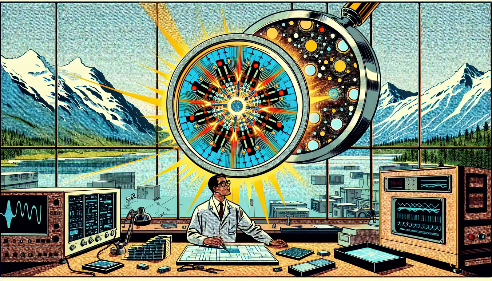
If you think the semiconductor industry is done shrinking transistors, think again. Norwegian startup Lace just closed a $40 million Series A round led by Atomico, with participation from Microsoft's M12 venture arm, to develop something that sounds like it belongs in a physics lab rather than a chip fab: helium atom beam lithography. The technology promises to etch chip features at scales 10 times smaller than the current state of the art — and if it works, it could reshape how the most advanced semiconductors on the planet are manufactured.
The current gold standard in chip lithography is extreme ultraviolet (EUV) technology, dominated by Dutch giant ASML. EUV uses light with a wavelength of 13.5 nanometers to print circuit patterns onto silicon wafers. Lace's approach replaces light with a focused beam of helium atoms that achieves a beam width of just 0.1 nanometers — a full two orders of magnitude finer than EUV. At that scale, you are not just making smaller transistors — you are working at the level of individual atoms.
The Science Behind the Beam
Lace was founded by Bodil Holst, a physicist from the University of Bergen in Norway, whose research in neutral atom beam technology forms the foundation of the company's approach. Unlike charged particle beams (such as electron beams), neutral helium atoms do not scatter or deflect when they interact with substrate materials, which allows for extraordinarily precise patterning without the damage that charged beams can cause to delicate semiconductor structures.
The practical advantage is resolution. While EUV lithography is approaching its physical limits — pushing to print features at 2 nanometers and below requires increasingly complex multi-patterning techniques — helium atom beam lithography operates at a resolution where those limitations simply do not apply. The beam can define features with atomic precision, opening the door to chip architectures that are not feasible with any existing lithography method.
Why Microsoft and Atomico Are Investing
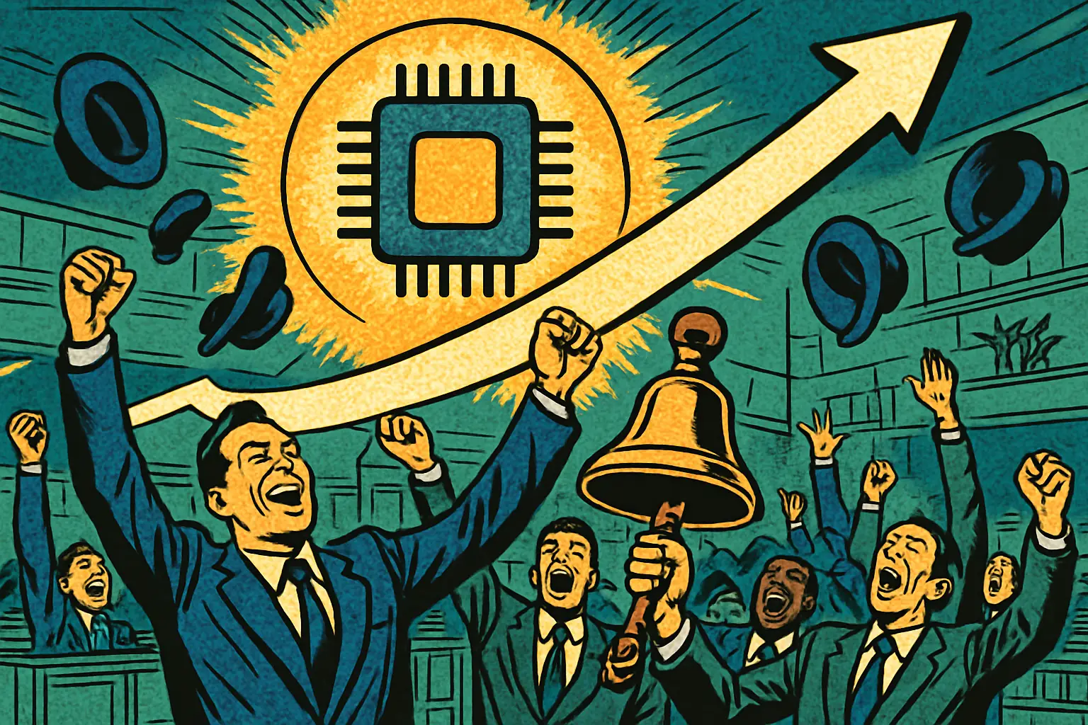
The $40 million Series A signals serious institutional confidence in the technology's commercial potential. Atomico, one of Europe's most prominent venture capital firms, led the round, bringing deep experience in scaling deep-tech startups. Microsoft's M12 participation is particularly interesting — Microsoft is one of the largest consumers of advanced semiconductors for its Azure cloud and AI infrastructure, giving the company a strategic interest in next-generation chip manufacturing technologies that could improve performance and reduce costs across its data centers.
The Road Ahead
Lace is targeting a pilot lithography tool installed in a production fab by 2029. That timeline reflects the reality that moving from laboratory-scale demonstrations to fab-ready manufacturing equipment is a multi-year engineering challenge. The company will need to prove that helium atom beam lithography can achieve the throughput, reliability, and cost characteristics that make it viable for high-volume semiconductor production — not just lab experiments.
For investors watching the semiconductor supply chain, Lace represents the kind of deep-tech bet that could pay extraordinary dividends if the technology scales. The global semiconductor lithography market is worth tens of billions of dollars annually, and any company that can offer a credible alternative or complement to ASML's EUV monopoly will attract enormous attention from chipmakers worldwide.
Sources: Tech Startups (March 23, 2026), BNN Bloomberg (March 23, 2026), The Next Web (March 23, 2026)
More Stock Trading Stories
SK Hynix IPO Becomes Biggest Foreign US Listing
SK Hynix raised $26.5 billion and closed up 13% on July 10, the largest US IPO ever by a foreign company, driven by AI memory demand.

Fincart's AI Wealth App Makes Goal-Based Investing Easy
Fincart's July 9 app update adds AI-powered, goal-based investing and bundles mutual funds, digital gold, and PMS to widen access for retail investors.

eToro's New AI-First App Adds Tori and Agent-Powered Portfolios
eToro rebuilt its app around AI, launching Tori — a proactive assistant on WhatsApp and Apple Watch — plus agent-powered portfolios that trade in dedicated sub-accounts.